World's Thinnest Transistor is Two-Thirds Complete

The high-tech devices of Silicon Valley depend on tiny, hard silicon chips. Yet in an imagined future in which walls, windows and clothes act as computing devices, the hardware components would have to be soft and flexible. One research group has taken a first step toward that flexible future, combining a conductor and an insulator in the thinnest sheet possible ? just one atom thick.
"This work shows that it is possible to bring together these two materials. What we believe that opens the doors to is the ability to create these atomically thin electronics, or more-complicated stacked electronics," said Mark Levendorf, a graduate student who worked on the new material. Levendorf studies nanotech chemistry at Cornell University.
"It's in the early phases," he added. "It's a step in the right direction toward miniaturizing things."
Transistors — the building blocks of all modern digital computers — require a conductor, an insulator and a semiconductor. Getting two of the three into the universe's thinnest sheet is a significant feat, said Chagaan Baatar, manager of the nanoscale electronics program at the Office of Naval Research, in Arlington, Va. [Ten Computers That Changed the World]
"This is the first time researchers have succeeded in patching together two different materials with vastly different electronic properties in the same two-dimensional (2D) sheet," he said in an email to InnovationNewsDaily.
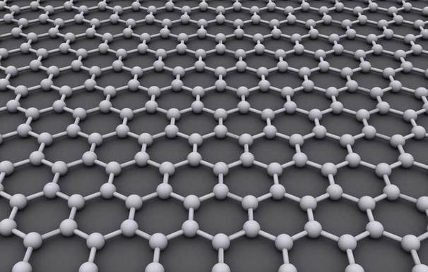
For its conductor, the new material uses graphene, a one-atom-thick sheet of carbon that carries electrons faster than any other chemical at room temperature. Because graphene is flexible and works much faster than silicon, many researchers think it will be a key supplement to silicon in the future. Because it's transparent, it also may go into touch screens. Labs around the world are studying how to put graphene into electronic devices.
Levendorf and his colleagues developed a technique to control exactly where they lay down the graphene and their insulator, boron nitride. With their specially patterned graphene and boron nitride, they created 1-centimeter- to 1-inch-long pieces of material through which they were able to run currents. Their tight control of where they arranged the graphene and the boron nitride meant they could direct currents in any way they wanted, which is important for building circuits, Levendorf said.
Sign up for the Live Science daily newsletter now
Get the world’s most fascinating discoveries delivered straight to your inbox.
They built up their sheet through a technique that's used in industry now, so it should be easy to create larger pieces of the graphene-boron nitride material, Levendorf said.
"That's another thing we're pretty excited about," he told InnovationNewsDaily. The Cornell lab was limited to 1-inch pieces because of its equipment, but other labs have the equipment to make larger pieces, he said.
Nevertheless, it may be a decade or longer before graphene transistors show up in people's laptops, Baatar said. The major hurdle to creating graphene-based computers is that it's impossible to stop the flow of current through graphene. That means researchers can't create transistors that turn on and off, which would be necessary to set up the logic questions that silicon digital devices use to operate.
"The challenge is formidable," Baatar said. But not impossible: "Unless you are violating some fundamental laws of nature, I would say nothing is impossible in science," he said, "particularly when it comes to a material as unique as graphene."
Adding a semiconductor to graphene would help. Levendorf and his colleagues are working on adding molybdenum disulfide to their material.
They published their work on their graphene-boron nitride sheet today (Aug. 29) in the journal Nature.
This story was provided by InnovationNewsDaily, a sister site to LiveScience. You can follow InnovationNewsDaily staff writer Francie Diep on Twitter @franciediep. Follow InnovationNewsDaily on Twitter @News_Innovation, or on Facebook.


