Fast and Ultra-Thin: Graphene Nanotransistors

This Behind the Scenes article was provided to LiveScience in partnership with the National Science Foundation.
Silicon has long been the workhorse of our digital world, but as silicon transistors shrink to the nanoscale, such factors as excessive power consumption in these devices could degrade performance.
"The scaling of silicon transistors has driven the economy around the world for the past half century," says Jeff Welser, director of the Nanoelectronics Research Initiative at the Semiconductor Research Corporation (SRC), a consortium made up of the world's largest semiconductor manufacturers. "The United States is the leader in microelectronics, and to maintain that leadership and to continue to drive the economy, we need to find a way to keep the device scaling going."
Many of the solutions being pursued around the world involve the adoption of new device architectures or new materials. Bhagawan Sahu, a research physicist at the Southwest Academy of Nanotechnology (SWAN), located at the University of Texas at Austin, is part of a nationwide search to find nanoscale materials and processes that can replace silicon transistors by the year 2020.
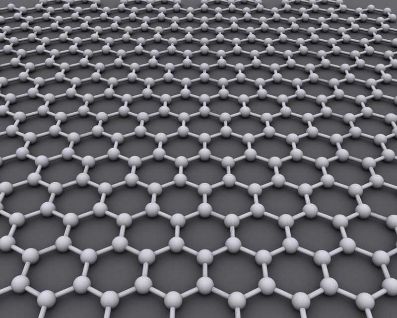
Sahu and his colleagues at SWAN aim to make transistors that are less than 10 nanometers long and less than one nanometer thick. To do so, they are exploring graphene, a single layer of graphite that is one of the thinnest materials in the world and possesses electron mobility (a measure of how fast electrons can move in response to external voltages) higher than silicon. Those characteristics are attractive features and have generated tremendous interest from the semiconductor industry.
After five years of dedicated study, the group’s novel, graphene-based design was selected by the SRC as one of only a handful of device ideas to be further studied.
"Understanding the device components [at the scale of atoms] through simulations has become [critical] for these nanoscale devices," Sahu says. "Our efforts at SWAN provide the community with the simulation results, which are obtained by virtual experiments before any real experiments are performed."
Sign up for the Live Science daily newsletter now
Get the world’s most fascinating discoveries delivered straight to your inbox.
The graphene-based system that the researchers created—which they call the bilayer pseudospintronic field-effect transistor (or BiSFET)—is based on two layers of graphene separated by a super-thin insulator of air or a vacuum. The physics of the device is based on “collective charge motion”, where a superfluid state forms at room temperature under certain conditions.
"In this structure, all of the electrons want to be in one layer or the other," Welser explains. "By applying a very small voltage—on the order of 25 millivolts—you can get all of the charge to jump from one side to the other. It acts like a switch, which is exactly how we want our transistors to act."
To explore this phenomenon, Sahu and his team used the NSF-supported Ranger and Lonestar 4 supercomputers at the Texas Advanced Computing Center (TACC). The computers, by virtue of their size and power, enabled the scientists to model new material systems that cannot be easily fabricated.
Moreover, the ability to simulate designs quickly and repeatedly allowed the researchers to experiment—virtually, with different widths, lengths, layer orientations, how layers are stacked and external voltages for graphene ribbons and flakes—to see how the variables influence the electronic properties, including the electron band gap, magnetism and other related factors. The simulations have been critical to understanding the internal and external variables that can affect device performance.
If the SWAN researchers can overcome the challenges involved in fabricating and demonstrating the BisFET devices, the nanotransistor may be the game changer that the semiconductor industry is betting on.
"The simulations are playing a major role in elucidating the interplay of the structure and the electronic properties of graphene," Sahu says. "We're building component by component, so we have an integrated view of what each part does and how it affects the whole device."
Editor's Note:The researchers depicted in Behind the Scenes articles have been supported by the National Science Foundation (NSF), the federal agency charged with funding basic research and education across all fields of science and engineering. Any opinions, findings, and conclusions or recommendations expressed in this material are those of the author and do not necessarily reflect the views of the National Science Foundation. See the Behind the Scenes Archive.


