Nanolasers on Silicon to Provide Faster Data Transmission

This Research in Action article was provided to Live Science in partnership with the National Science Foundation.
Fiber optic networks play a key role in transmitting feature films to laptops, cool apps to smartphones and lifelike video games to game consoles. To ensure networks keep up with consumer demand for speed and seamless data flow, researchers continue to pursue new combinations of electronic and optical devices.
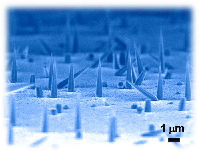
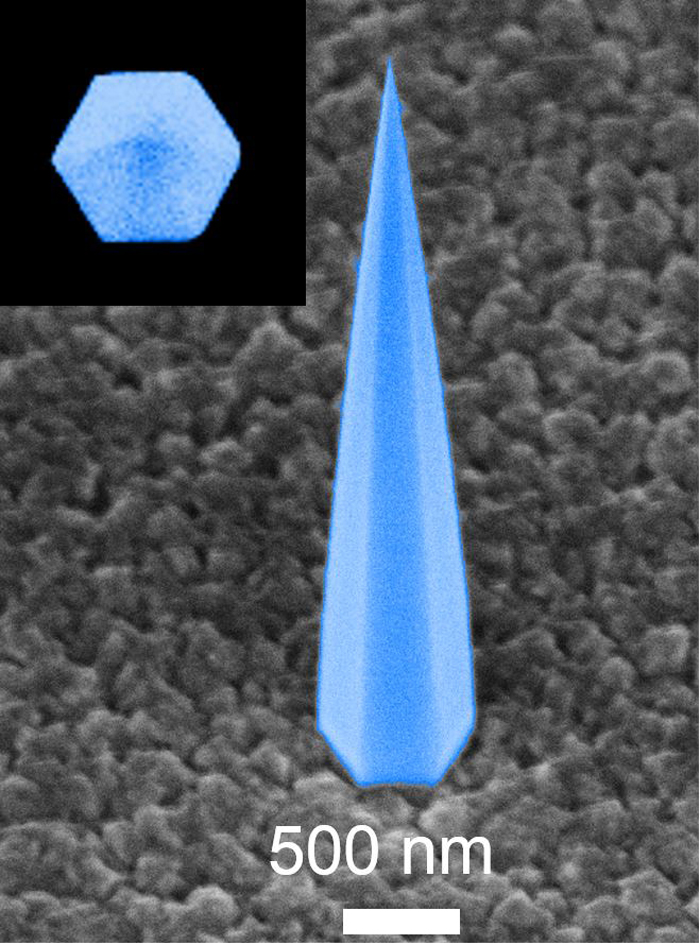
One promising approach involves growing lasers on silicon , the base layer of choice for electronic devices. The lasers, called nanoneedles, are just one-tenth the width of a human hair and were developed by researchers working at the University of California, Berkeley. By growing lasers on silicon wafers, the researchers are expanding the ability of electronics to transmit data at capacities required by next-generation consumer devices and systems. [Fiber Optics Could ‘Humanize’ Future Prosthetic Limbs ]
“On any given integrated circuit now, the electrical power dedicated for communication is really high and bandwidth limited, especially for higher speed trunk lines,” says Connie Chang-Hasnain, who leads the effort. Optical approaches such as lasers reduce power consumption and noise between components and increase speed, she says. "It’s the difference between using a local roadway and a superhighway.”
To combine the strengths of silicon and optical laser materials, the Berkeley researchers overcame two longstanding challenges that have vexed researchers: 1) the mismatch between the crystalline structures of silicon and III-V semiconductor material, an essential solid-state laser material, and 2) growth temperatures that are incompatible with current integrated circuit fabrication.

During the 10- to 15-minute crystal growth process, which occurs at temperatures between 400° and 450° C, nanoneedles in the shape of hexagonal pyramids emerge from a silicon base. These high-quality crystals can reach several hundred nanometers and can be layered, doped (i.e., other materials can be added to the crystal during the growth process, resulting in a crystal that has additional properties) or etched to create laser structures for device applications. The nanoneedle geometry provides a natural laser cavity that traps light by circulating it up and down the inside of the nanoneedle in a helical fashion.
Chang-Hasnain notes that the growth process and use of silicon as a growth medium will make large-scale manufacturing possible when the nanoneedles are ready for commercial use. The strong investment by the electronics industry in a silicon foundry network will enable development of nanolasers for communications as well as other applications such as solar energy and sensing.
Sign up for the Live Science daily newsletter now
Get the world’s most fascinating discoveries delivered straight to your inbox.
The nanoneedle research is supported in part by the Center for Integrated Access Networks, an NSF-funded Engineering Research Center headquartered at the University of Arizona.
Editor's Note: Any opinions, findings, and conclusions or recommendations expressed in this material are those of the author and do not necessarily reflect the views of the National Science Foundation. See the Research in Action archive.


