This Tiny Electronic Chip Is Just 3 Atoms Thick

A tiny electronic chip just three atoms thick could yield advanced circuits that are powerful, flexible and transparent, researchers said in a new study. The scientists said the chip demonstrates a new way to mass-produce atomically thin materials and electronics.
These materials could be used to develop electronic displays on windows or windshields, along with powerful microchips in which circuitry spreads not just two-dimensionally but also rises three-dimensionally, the researchers said.
For more than 50 years, silicon has been the backbone of the electronics industry. However, as silicon transistors reach the limit of miniaturization, scientists worldwide are investigating new materials that could serve as the foundation of even tinier devices. [10 Technologies That Will Transform Your Life]
In the past decade or so, researchers discovered that atomically thin materials could serve as the basis of electronic devices. For instance, sheets of graphene — a material related to the "lead" in pencils — are each just one carbon atom thick. Graphene is an excellent conductor of electricity, making it ideal for use in wiring.
However, previous research found that graphene is not a semiconductor, whereas silicon is. This means that graphene cannot easily be used in transistors, the microscopic switches that lie at the heart of electronic circuits. A semiconductor can act either as a conductor or insulator to enable or disable the flow of electricity. Transistors are typically made of semiconductors, relying on the properties of these materials to flick on and off to symbolize bits of data as digital ones and zeroes.
Instead of graphene, therefore, some researchers are exploring molybdenite, or molybdenum disulfide (MoS2), for use in advanced electronics. Molybdenum disulfide is a semiconductor, and the new study finds that molybdenum disulfide transistors "can be switched on and off significantly better than graphene and somewhat better than silicon," said study senior author Eric Pop, an electrical engineer at Stanford University in California.
Moreover, films of molybdenum disulfide can be as thin as only three atoms, each consisting of a sheet of molybdenum atoms sandwiched between two layers of sulfur atoms. A single-molecule layer of molybdenum disulfide is only six-tenths of a nanometer thick. In contrast, the active layer of a silicon microchip is up to about 100 nanometers thick, Pop said. (A nanometer is a billionth of a meter; the average human hair is about 100,000 nanometers wide.)
Sign up for the Live Science daily newsletter now
Get the world’s most fascinating discoveries delivered straight to your inbox.
These single-molecule-thin chips would be not only flexible, but also transparent. "What if your window was also a television, or you could have a heads-up display on the windshield of your car?" study lead author Kirby Smithe, an electrical engineer at Stanford University, said in a statement.
Scientists have struggled to find ways to mass produce extraordinarily thin layers of materials such as graphene and molybdenum disulfide. For example, initial experiments with graphene involved ripping layers of the material off a rock using sticky tape, a messy technique likely of no practical use in large-scale manufacturing, Pop said.
Now, Pop and his colleagues have developed a new strategy to mass produce molybdenum disulfide chips. "We finally don't have to rely on the Scotch-tape method of producing these extraordinarily thin materials," Pop told Live Science.
To create their ultrathin chip, the scientists incinerated small amounts of molybdenum and sulfur and then used the resulting vapor to form molecule-thin layers of molybdenum disulfide on a variety of surfaces, such as glass or silicon. "We went through a lot of painstaking trial and error to find the right combination of temperature and pressure to help grow these layers in a repeatable manner," Pop said.
Using this new technique, the researchers manufactured single-molecule-thick molybdenum disulfide chips measuring about 0.06 inches (1.5 millimeters) wide. These chips are each about 25 million times wider than they are thick, the researchers said.
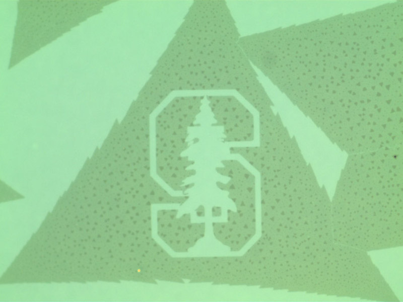
To show how circuits might get etched onto these single-molecule-thick chips, the scientists used electron beams to carve the Stanford University logo onto the molybdenum disulfide films. The researchers also etched portraits of the two major-party candidates in the 2016 U.S. presidential election, Hillary Clinton and Donald Trump.
"Perhaps seeing portraits etched into a three-atom-thick canvas will inspire future researchers in ways we can't even imagine yet," Pop said in a statement.
The scientists will now focus on ways to make these films uniform across their entirety, and on building actual circuits from them, Pop said. "We can imagine putting molybdenum sulfide layers onto silicon layers, to build microchips vertically instead of just horizontally," Pop said. "It would be much easier to shuffle energy around such 3D architectures than conventional flat architectures."
Further studies could also explore ways to delicately remove molybdenum disulfide layers from the surfaces on which they are manufactured and transfer them onto materials such as cloth or paper. One strategy for doing this might involve a relatively well-known industrial process that would coat the single-molecule-thin film with a sticky, flexible plastic polymer and then gently peel this combination off a surface.
"This sounds a lot like using Scotch tape, but it'd involve uniform polymer films that can be peeled off with constant force in an automated and much more controlled way," Pop said.
The scientists detailed their findings online Dec. 1 in the journal 2D Materials.
Original article on Live Science.


