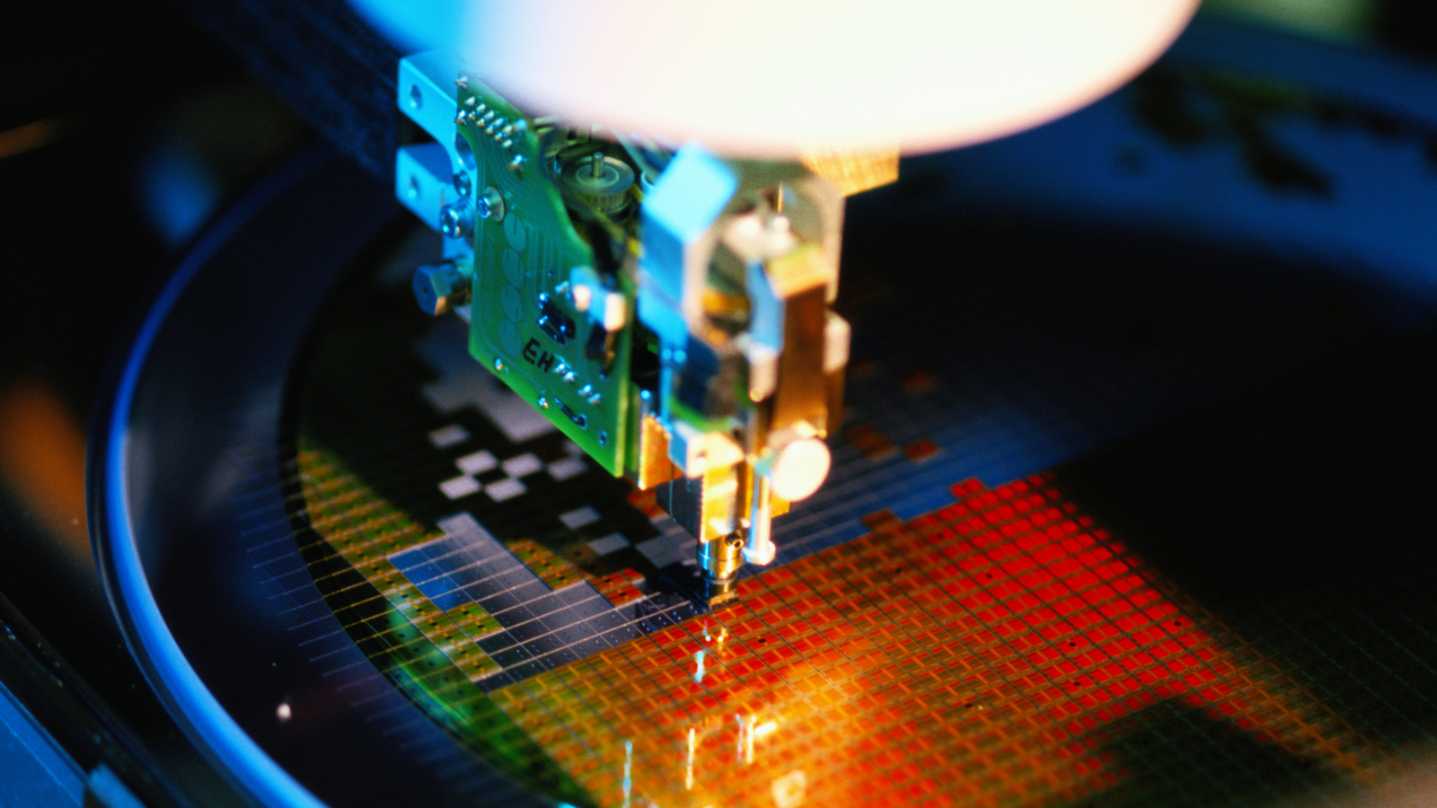
'Defects' in silicon chips could house qubits, hastening the arrival of a future quantum internet
Using manufacturing defects in silicon chips to house signal-amplifying qubits could help to usher in the much-anticipated quantum internet.

Get the world’s most fascinating discoveries delivered straight to your inbox.
You are now subscribed
Your newsletter sign-up was successful
Want to add more newsletters?
Join the club
Get full access to premium articles, exclusive features and a growing list of member rewards.
Researchers in quantum mechanics believe they’ve found a standard way to assess the viability of quantum memory in silicon chips — meaning existing components can be used as the fabric for a future quantum internet.
This discovery comes on the heels of several other findings in the quantum networking realm, bringing a working network that connects quantum computers a step closer to reality. The biggest barrier is providing a dependable structure for carrying quantum data from one area to another.
"It’s still a Wild West out there,” said lead researcher Evelyn Hu, professor of applied physics and electrical engineering at Harvard University, in a statement. "Even though new candidate defects are a promising quantum memory platform, there is often almost nothing known about why certain recipes are used to create them, and how you can rapidly characterize them and their interactions, even in ensembles."
Article continues belowThese new candidate defects are found in silicon chips as a result of the manufacturing process. Hu and her team set out to discover ways to measure and control the performance of qubits in "G-center" defects in silicon chips, and how G-centers perform when interacting with electric fields.
G-centers are carbon-based defects in silicon, while T-centers are carbon and hydrogen-based defects. Both are used in telecommunications to facilitate transmission of O-bands — a wavelength band used in the infrared light for optical communications.
The application of G-centers and T-centers in quantum networking helps solve a common problem in quantum computing: stabilization of wavelengths. Hu’s team focused on G centers for the purpose of this study.
Get the world’s most fascinating discoveries delivered straight to your inbox.
While G-centers are usually created with only carbon atoms, the researchers found adding a hydrogen atom allowed for consistent fabrication of the defect. The team also explored how to control the behavior of G-centers to generate the desired properties.
"If we are ever to make a technology out of this wide world of possibilities, we must have ways to characterize them better, faster and more efficiently," said Hu.
The team successfully controlled the G-center quantum emitter by using electrical diodes that surround the defect at the center of a silicon wafer without sacrificing the desired wavelength outputs.
This allowed the team to turn the defects on and off by applying either negative or positive voltage. They found local electric fields created a more stabilized wavelength output, which is critical to the successful implementation of quantum networking of different systems.
Finally, Hu’s team developed a system to monitor, diagnose and track the defects, giving them useful data to inform future research into creating ideal environments for defects. The team also hopes to use the same techniques to beter understand T-center defects in silicon.
Lisa D Sparks is a freelance journalist for Live Science and an experienced editor and marketing professional with a background in journalism, content marketing, strategic development, project management, and process automation. She specializes in artificial intelligence (AI), robotics and electric vehicles (EVs) and battery technology, while she also holds expertise in the trends including semiconductors and data centers.
 Live Science Plus


